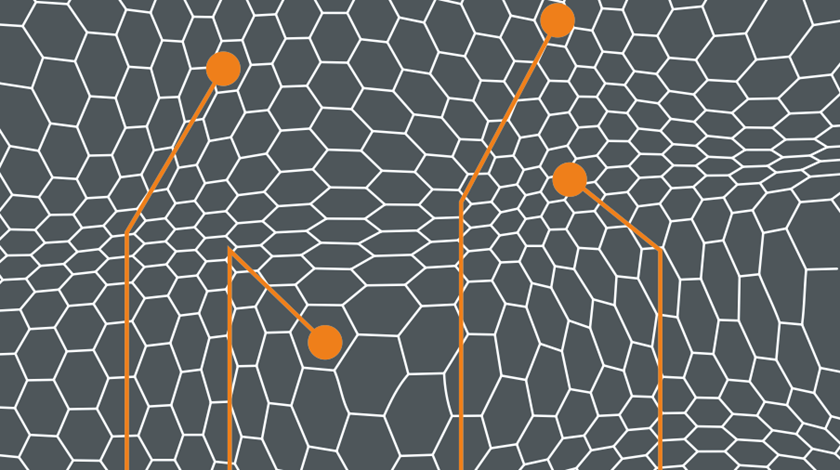
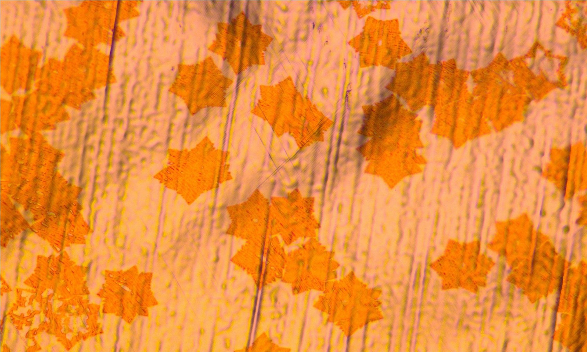
Researchers from RWTH Aachen University and the Graphene Flagship Standardization Committee have pushed through a new IEC standard for assessing the strain uniformity of single-layer graphene using Raman spectroscopy.
Graphene is often portrayed as the “ultimate conductor”, thanks to its flexibility and to its excellent conductivity. However, research has shown that the electrical and the structural quality of graphene are intimately connected, and that nanoscale lattice deformations caused by surface corrugations are a major factor that limits the mobility of electrons in graphene. The flatness of the graphene sheet is therefore a key control characteristic for the fabrication of high-quality graphene layers for electronic devices – and the possibility of measuring it with a simple and fast method is a major technological advantage.

The method in question is Raman spectroscopy. This is a standard tool of graphene research, as it is fast, non-destructive and well understood, especially if the samples under evaluation consists of single-layer graphene. It allows distinguishing between graphene and few-layer graphene, as well as it can be used to determine the doping of a graphene sample and the amount of mechanical strain and defects in the lattice [1,2]. Furthermore, in 2015 the group of Christoph Stampfer at RWTH Aachen University was able to show that Raman spectroscopy contains also unambiguous information on the amount of nanometer-scale strain variations in a graphene sheet, i.e. on its flatness [3].
This insight came at a very appropriate time, as nanometer-scale strain variation had been pinpointed as the main source of electron scattering in defect-free graphene just the year before [4]. “It was clear that the result of the RWTH group had the potential for setting the basis of an internationally recognized standard for the strain uniformity of graphene”, says Dr. Norbert Fabricius, from International Standards Consulting GmbH & Co. KG.
Fabricius, who at the time was Chairman of the Graphene Flagship Standardization Committee (GFSC), is one of the initiators of the long process that brings from a scientific discovery to an international standard. The big bulk of work necessary to establish the standard was performed in group of Christoph Stampfer. The result is a well-defined recipe to use scanning confocal Raman mappings to produce a “strain uniformity parameter” based on the statistical interpretation of the linewidth of the 2D-peak (one of the characteristics Raman peaks of single layer graphene) [5].
“The strain uniformity parameter is a figure of merit that quantify the influence of nanometer-scale strain variations on the electronic properties of the layer. It gives an upper limit on the electronic performance of the characterized graphene. It can therefore help manufacturers to classify their material and decide whether or not it is potentially suitable for various applications”, explains Fabricius.
The standard has been published by the International Electrotechnical Commission (IEC) in October 2021, and represents a good example of the work supported by the Graphene Flagship Standardization Committee (GFSC), now chaired by Thurid Gspann from Karlsruhe Institute of Technology (KIT). “A standard must meet the different needs of different stakeholders – researchers, manufacturers, and buyers”, says Gspann. “In the Committee we mediate the discussion between different actors to find consensus on the specifications of the standard, we support the scientific work that forms the backbone of the standard, and we link to international organization such as the International Organization for Standardization (ISO) or, in this case, the International Electrotechnical Commission (IEC).”
The scientific work was in this case carried out at RWTH Aachen University, in the group of Christoph Stampfer, who says: “In my view, the largest portion of merit in this story goes to two PhD students from my group, Christoph Neumann, who realized the potential of Raman spectroscopy to measure nanometer-scale strain fluctuations and who initiated the work needed for the standard. And Jens Sonntag, who picked up the work initiated by Christoph and pushed it until the very final stage.” As appreciation for they work, Stampfer, Neumann and Sonntag have received the “GFSC standardization certificate” for authoring an international standard on graphene.
“Established standards can increase efficiency, reduce risks and costs, and catalyze innovation”, says Gspann. “This particular standard will allow manufacturers to certify that their material is in principle suitable for applications that crucially depend on the electronic quality of graphene, such as high-frequency transistors and broad-band receivers. This can accelerate the appearance of this type of devices onto the market.”
Kari Hjelt, Head of Innovation of the Graphene Flagship, adds: “The Graphene Flagship devotes most of its resources to commercializing graphene-enabled products. That requires both reliable materials and solutions and industry trust, both of which are boosted by international standards, like the one just granted to Stampfer’s method to measure the flatness of graphene. I am convinced the work of our Graphene Flagship Standardisation Committee will keep bearing fruits and ultimately speeding up the early adoption of graphene and related materials.”
References
[1] A. Jorio, R. Saito, G. Dresselhaus, M. S. Dresselhaus, „Raman Spectroscopy in Graphene Related Systems”, Wiley-VCH Verlag GmbH (2011).
[2] A. C. Ferrari, D. M. Basko, “Raman spectroscopy as a versatile tool for studying the properties of graphene”, Nature Nanotechnology 8, 235 (2013).
[3] C. Neumann, S. Reichardt, P. Venezuela, M. Drögeler, L. Banszerus, M. Schmitz, K. Watanabe, T. Taniguchi, F. Mauri, B. Beschoten, S. V. Rotkin, and C. Stampfer, “Raman spectroscopy as probe of nanometer-scale strain variations in graphene”, Nature Communications 6, 8429 (2015).
[4] N. J. G. Couto, D. Costanzo, S. Engels, D.-K. Ki, K. Watanabe, T. Taniguchi, C. Stampfer, F. Guinea, A. F. Morpurgo, “Random Strain Fluctuations as Dominant Disorder Source for High-Quality On-Substrate Graphene Devices”, Phys. Rev. X 4, 041019 (2014).
[5] IEC TS 62607-6-6 “Nanomanufacturing – Key control characteristics – Part 6-6: Graphene – Strain uniformity: Raman spectroscoopy” https://webstore.iec.ch/publication/34162.
