A review article on one of the most delicate issues of future electronics based on 2D materials
A team of scientists led by Tibor Grasser and Yuri Illarionov of TU Wien, including RWTH Professor and AMO Director Max Lemme, has published an extensive review of the current search for suitable insulators for two-dimensional (2D) nanoelectronics in Nature Communications.

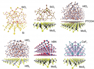
Insulators play a crucial but often forgotten role in electronic devices. The performance and reliability of field-effect transistors (FETs) and other electronic devices depends critically on the quality of the insulator that separates the gate electrode from the transistor channel, and on the interface the insulator form with the channel. This became very apparent when the semiconductor industry searched for a solution to replace the standard silicon dioxide with novel “high-k” dielectrics that would enable further scaling along with Moore’s law. Years of research and millions of Euros were spent to change the gate insulator “at the heart of the transistor”.
In the field of 2D materials, many investigations have focused on the physical and electrical properties of the 2D materials that form the transistor channel. Nevertheless, this field eventually faces the same challenges as conventional semiconductors. Theoretical calculations predict excellent properties for devices build from 2D semiconductors such as MoS2 and other transition metal dichalcogenides (e.g. MoSe2, MoTe2, WS2, WSe2) or black phosphorus. But the devices realized so far suffer often from non-competitive carrier mobilities, subthreshold swings, and drifts of important device parameters that arise from the gate insulators used. The result is that there is still no commercially-competitive 2D-transistor technology available today.
“Already in 2006, I wrote in a proposal that the most important aspect for the usability of graphene in electrical devices is the possibility of passivation, and this is still true today”, says Max Lemme. “In fact, this statement must now be extended to other 2D materials. We need to find suitable insulators that allow retaining the original electrical properties of the 2D materials, even after sealing with an insulating layer.”
The review presents the current state-of-the-art regarding gate insulators for 2D technologies and discusses strategies for further improving the performance of 2D devices – like the creation of clean interfaces, the production of native oxides from 2D semiconductors and more intensive studies on crystalline insulators. While the main focus of the review is on standard 2D FETs, the problems addressed are directly relevant also for alternative device technologies, such as tunnel FETs, ferroelectric FETs, negative-capacitance transistors and analog field-effect devices (e.g. photodetectors and biosensors).
“The solution to the quest for a suitable insulator will be crucial for the commercial uptake of any semiconductor-related application of 2D materials, be it electronics, photonics or sensors”, says Lemme. “We will therefore address this issue in the forthcoming Graphene Flagship’s 2D Experimental Pilot Line, funded by the European Commission”.
Bibliographic information:
“Insulators for 2D nanoelectronics: the gap to bridge”
Y. Y. Illarionov, T. Knobloch, M. Jech, M. Lanza, D. Akinwande, M. Vexler, T. Mueller, M. C. Lemme, G. Fiori, F. Schwierz & T. Grasser, Nat Commun 11, 3385 (2020).
https://doi.org/10.1038/s41467-020-16640-8
Contact:
Prof. Max C. Lemme
lemme@amo.de
