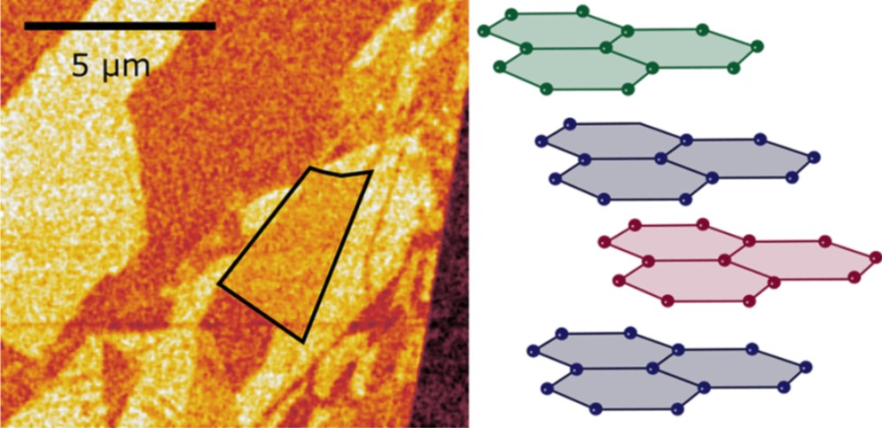
Using advanced spectroscopic techniques, researchers from RWTH Aachen University have been able to observe for the first-time domains of tetralayer graphene with ABCB stacking. The results have been reported in ACS Nano.

According to theory, there are three inequivalent ways of stacking four layers of graphene on top of each other: Bernal stacking (ABAB), which is the most energetically favorable configuration, rhombohedral stacking (ABCA), and a third metastable ordering labeled ABCB. These three crystallographic configurations exhibit remarkably different electronic and optical properties. In particular, ABCB tetralayer graphene is expected to be the thinnest graphene-based band insulator, and to present flat bands around the K points, which makes it a very interesting system for studying correlated states. Until now, however, the ABCB stacking has eluded the experimental observation.
“The stacking order in few-layer graphene can be determined using different optical techniques, such as Raman spectroscopy or infrared absorption. However, these methods are limited in spatial resolution by diffraction, and are therefore prone to oversee small domains. That’s why we started a collaboration with the group of Prof. Thomas Taubner at RWTH, which has a unique tool for near-field infrared spectroscopy with a resolution down to 20 nm.” explains Professor Christoph Stampfer, one of the authors of the paper.
The tool is a scattering-type scanning near-field optical microscope (s-SNOM), which allows to probe the stacking-specific optical conductivity of few layer graphene with sub-diffraction resolution. The measured data agree very well with the theoretical predictions calculated by the group of Prof. Dante Kennes, also at RWTH, allowing to assign unambiguously the ABCB domains. The assignment is further confirmed by measurements of the Raman G, 2D, and M peaks of all three stacking orders, which constitutes a second, independent means of identifying the three different domains.
Regarding the abundance and the stability of the ABCB domains, during the work approximately 40000 μm2 of tetralayer graphene have been investigated, and only about 2 % of the total area presented ABCB domains – the largest approximately 100 μm2 in size – which can explain why then haven’t been reported before. On the other hand, the ABCB domains were stable over the course of several weeks at ambient conditions as well as when subjected to SNOM and Raman measurements at moderate laser powers.
“Even if the ABCB domains are probably not very relevant from the application point of view, they are extremely interesting in terms of fundamental physics, as they can host exotic correlated phases of matter”, says Stampfer. “Our work represents a convenient starting point for further investigations.”
Bibliographic information
“Experimental Observation of ABCB Stacked Tetralayer Graphene”
K. G. Wirth, J. B. Hauck, A. Rothstein, H. Kyoseva, D. Siebenkotten, L. Conrads, L. Klebl, A. Fischer, B. Beschoten, C. Stampfer, D. M. Kennes, L. Waldecker, and T. Taubner
ACS Nano 2022 (advanced online publication)
https://doi.org/10.1021/acsnano.2c06053
