A scalable method to reduce the contact resistance of graphene

The exceptional electronic properties of graphene make it a material with large potential for low-power, high-frequency electronics. However, the performance of a graphene-based device depends not only on the properties of the graphene itself, but also on the quality of its metal contacts. The lack of effective and manufacturable approaches to establish good ohmic contacts to a graphene sheet is one of the factors that limit today the full application potential of graphene technology.
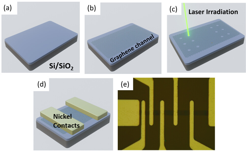
(a–d) Schematics showing the process sequence for manufacturing the devices and the laser irradiation of graphene in the contact regions. (e) Optical micrograph of one of the measured devices
Continue reading “A scalable method to reduce the contact resistance of graphene”

A non-destructive way to probe inter-layer coupling on millimeter-scale graphene-MoS2 heterostructures

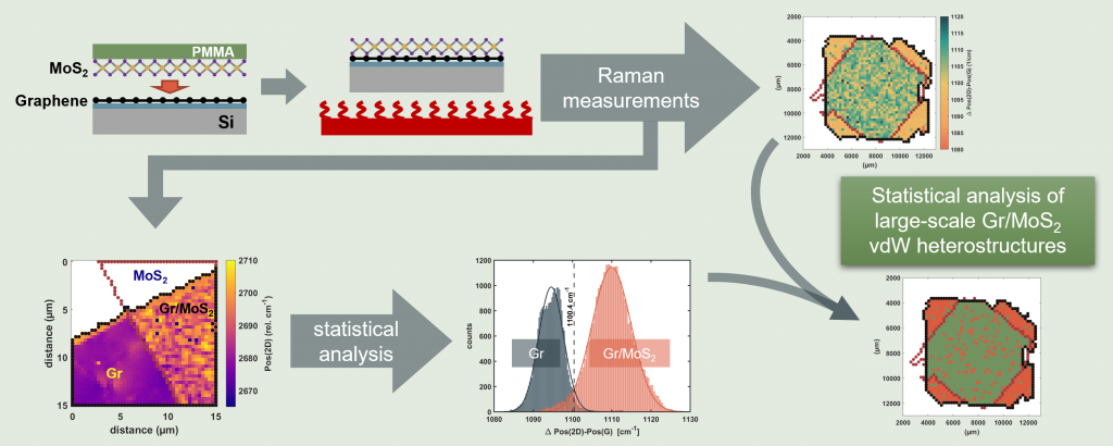
One of the great assets of two-dimensional (2D) materials is the possibility of placing different materials on top of each other to form heterostructures with properties tailored to specific application scenarios. However, the quality of the final material stack strongly depends on the electronic coupling between the different materials. Measuring this coupling in a non-destructive way is therefore an important aspect for material development. Researchers from AMO GmbH, RWTH Aachen University and AIXTRON SE have now established a methodology based on Raman spectroscopy for estimating quantitatively the coupling between graphene and molybdenum disulfide (MoS2) in heterostructures up to the mm2-scale.

Graphical summary of the work of Nico Rademacher and co-workers (From: Micro and nano Engineering, https://doi.org/10.1016/j.mne.2024.100256)
Continue reading “A non-destructive way to probe inter-layer coupling on millimeter-scale graphene-MoS2 heterostructures”

An effective method to measure the adhesion of 2D materials

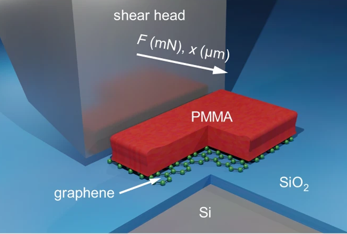
One of the big selling points of two-dimensional (2D) materials is their self-passivated nature, which allows them to be deposited on any substrate and opens up new possibilities for three-dimensional material stacks. The downside is their weak adhesion to the substrate, which can be a source of device instability. Quantifying the adhesion of 2D materials to three-dimensional surfaces is therefore an essential step for the reliable integration of devices based on 2D materials. A team of researchers around Max Lemme has now shown that the adhesion between 2D materials and substrates can be efficiently quantified using button-shear testing.

Schematic representation of the working principle of button shear testing.
Continue reading “An effective method to measure the adhesion of 2D materials”

An automatic flake-search tool for 2D materials

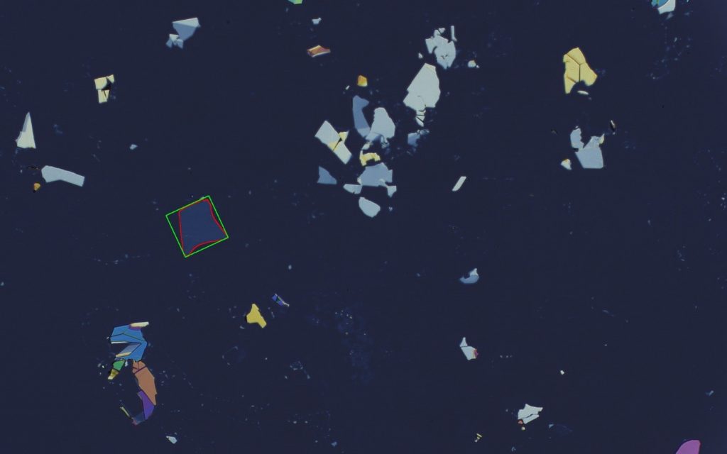
Researchers at the Aachen Graphene & 2D Materials Center have released an open-source platform to automatically identify and classify exfoliated flakes of two-dimensional (2D) materials on a substrate, shortening one of the most time-consuming and tedious tasks in the study of 2D materials.

Exfoliated flakes of hexagonal Boron Nitride (hBN) on Si/SiO2 substrate. The red contour indicates a flake with a thickness of about 5 nanometers and size of approximately 50µm x 50µm.
Continue reading “An automatic flake-search tool for 2D materials”

First observation of coherent charge dynamics in graphene quantum dots

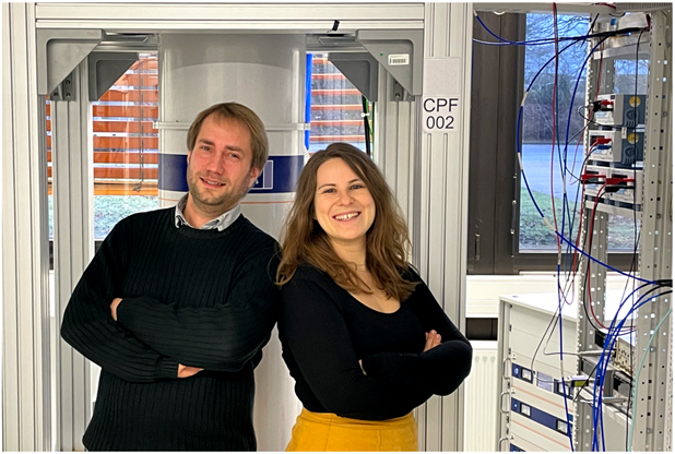
In a recent study published in Nature Communications, researchers from RWTH Aachen University and Forschungszentrum Jülich have reported the observation of coherent charge oscillations in bilayer graphene quantum dots. This marks a significant milestone on the way to spin and valley qubits in a two-dimensional material system.

Katrin Hecker (right), Christian Volk (left) and colleagues from RWTH Aachen University have realized the first “charge qubit” in bilayer graphene, marking a significant milestone on the way to spin and valley qubits in a two-dimensional material system. (Photo: Hubert Dulisch/RWTH Aachen University)
Continue reading “First observation of coherent charge dynamics in graphene quantum dots”

High quality hexagonal Boron Nitride – made in Aachen

Good news for the community working on two-dimensional materials in Europe: a team of researchers at RWTH Aachen University has successfully implemented the process for growing high-quality hexagonal Boron Nitride at atmospheric pressure and high temperature, increasing the resilience of the supply chain of this unique material.

Hexagonal Boron Nitride grown in Aachen: the growth process results in a continuous crystal-layer with crystal grains of the order of a few 100 µm.
Continue reading “High quality hexagonal Boron Nitride – made in Aachen”

Interlayer transfer of valley polarization from excitons to free charge carriers in WSe2/MoSe2 heterobilayers

Scientists from RWTH Aachen, AMO GmbH, Forschungszentrum Julich and the University of Regensburg have shown that in twisted heterobilayers of WSe2 and MoSe2 there is a transfer of valley polarization from excitons in WSe2 to free carriers in MoSe2. This mechanism, which is strongly dependent on the twist angle, may allow the realization of opto-valleytronic devices where the valley polarization is optically excited but extracted and measured by electrical means. The results are reported in npj 2D Materials and Applications.

Cover image on 2D materials and applications. Image credits: Sebastian Staacks.
Continue reading “Interlayer transfer of valley polarization from excitons to free charge carriers in WSe2/MoSe2 heterobilayers”

Near perfect particle-hole symmetry in graphene quantum dots

Researchers at RWTH Aachen University and Forschungszentrum Jülich have uncovered important characteristics of double quantum dots in bilayer graphene, an increasingly promising material for possible applications in quantum technologies. The team has demonstrated near-perfect particle-hole symmetry in graphene quantum dots, which could lead to more efficient quantum information processing. The study has been published in Nature.  

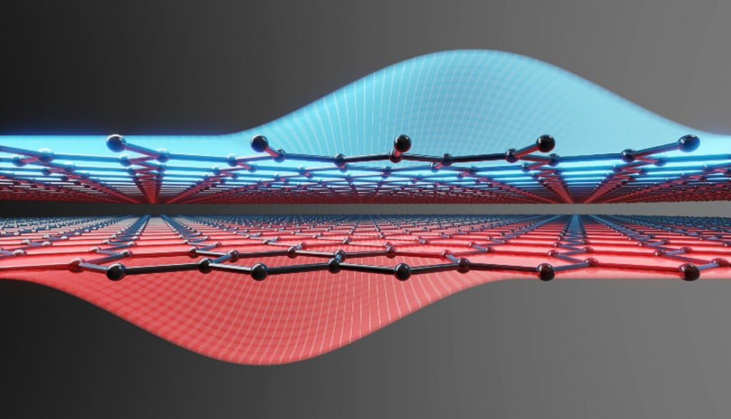
Artist impression of bilayer graphene hosting a symmetric electron-hole double quantum dot, where the electron and hole are located on the different layers. Credit: Sebastian Staacks
Continue reading “Near perfect particle-hole symmetry in graphene quantum dots”

A scalable pathway for the mechanical transfer of graphene grown by CVD 

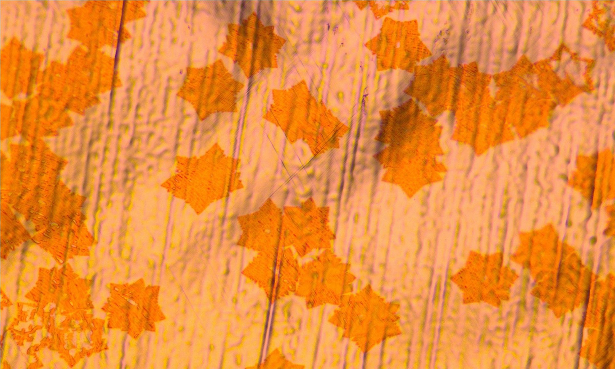
Nowadays it is possible to grow high-quality graphene on large scale using chemical vapor deposition (CVD). What remains a major bottleneck for the industrialization of the material is the transfer of graphene from the growth substrate to a target one. A team of researchers from the University of Cambridge and RWTH Aachen University has now developed a methodology for optimizing simultaneously the growth and the transfer process, showing that it is possible to dry-transfer graphene with high-yield, if the crystallographic orientation of the growth surface is chosen appropriately.

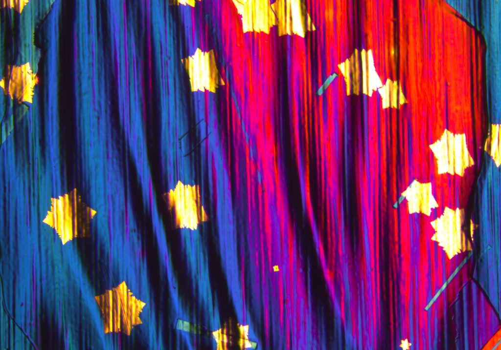
Optical micrograph of star-shaped graphene flakes grown by CVD on copper.
(© Stampfer Lab, RWTH Aachen University) 
Continue reading “A scalable pathway for the mechanical transfer of graphene grown by CVD “

First experimental observation of an elusive stacking order in tetralayer graphene

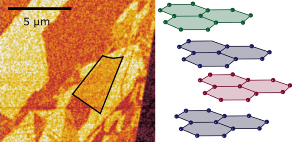
Using advanced spectroscopic techniques, researchers from RWTH Aachen University have been able to observe for the first-time domains of tetralayer graphene with ABCB stacking. The results have been reported in ACS Nano.

s-SNOM imaging of different stacking domains in tetralayer graphene. The highlighted domain and schematics on the right correspond to ABCB stacking .
Continue reading “First experimental observation of an elusive stacking order in tetralayer graphene”